


Unique products created with patented technologies
Exosens Imaging professional imaging and photodetection products are based on unique technologies that integrate nanostructured optical absorbers, graphene transducers and in-house designed CMOS circuitry.
Exosens Imaging has developed a library of material solutions that enable creation of photodetectors for the full spectral range from visible to long-wavelength infrared radiation. Selected material solutions enable monolithic integration on the top surface of CMOS wafers.
Our team has created more than 100 patent applications in related technologies and we have a steadily growing IP portfolio. Our ground-breaking work has been reported in numerous publications in high-impact scientific journals.
Exosens Imaging's innovation in the integration of CMOS electronics with novel nanomaterials including the design and fabrication process creates a unique value chain to create a highly efficient and scalable technology solution.
- Innovative pixel structure
- Patented measurement techniques and modes
- CQD – Graphene Photodiode Device architecture
- Custom ROIC design for scalable pixel design up to 4K HD
Nanomaterials and Radiation Absorbers
Exosens Imaging's knowhow of integrating optically absorbing materials with graphene transducers provides a versatile way of creating sensors and detectors on CMOS ROIC substrates for diverse applications. Exosens Imaging has optimised various processes and has developed device sensor structures using nanomaterials such as colloidal quantum dots and graphene.
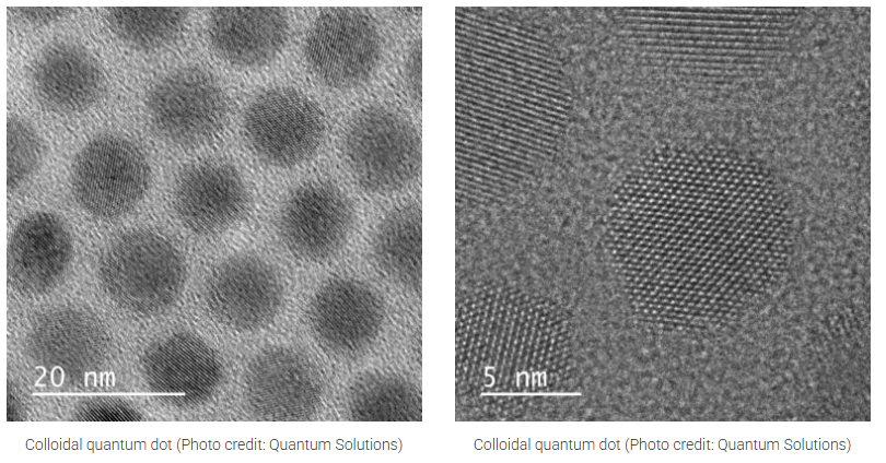
Colloidal quantum dot image sensors diverge from conventional image sensors:
- Colloidal quantum dot (CQD) devices are produced using wet chemistry, which make their processing inexpensive and highly scalable.
- Their wavelength range of photon absorption can be tuned and be made very broad.
- Even the quantum efficiency of CQD devices is typically lower, the low noise of the CQD photodiodes compensates it and the noise equivalent power (NEP) is sufficient for most of the applications.
- CQD SWIR image sensors can be operated at higher temperatures, reducing the system and sensor packaging cost.
- Based on possible direct monolithic integration on CMOS wafers, CQD pixels are scalable to small pixel size and high image resolution formats, e.g., up to 4K HD format.
- Exosens Imaging can scale its pixel arrays either down to very small pixel sizes or larger sizes depending on the application needs.
Superior SWIR technology
Exosens Imaging has developed sensor device structures and manufacturing methods combining nanocrystalline optical absorbers with graphene-based transistors, enabling photodetection from visible (VIS, 400 nm) leading to extended SWIR 2000 nm and ultimately to 2500 nm wavelengths.
Exosens Imaging's investments are focused on differentiating manufacturing processes: photodiode processing, sensor packaging, camera assembly, testing, and calibration.
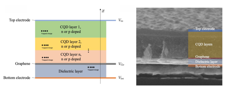
Our semiconducting nanocrystalline material enables convenient fabrication directly on standard CMOS wafers. Compared to the hybrid packaging processes required for competing semiconductor heterosubstrate-based transducers, this is a major advantage that leads to improved yield, increased reliability and lower manufacturing costs.
Exosens Imaging employs different colloidal quantum dot materials that can be integrated reliably on graphene transducers and tailored to meet specific wavelength range and response curve requirements.
Graphene – 2D Layered Materials
Use of 2D graphene in image sensor pixels enables extreme simplification of the fabrication process together with significant improvements in noise performance and stability, enabling operation at higher temperatures.
Exosens Imaging's technology can be utilised with highly sensitive graphene transducers, which detect the electric charge generated in surrounding materials and convert the original optical signal into an electrical signal via a high-gain amplification mechanism.
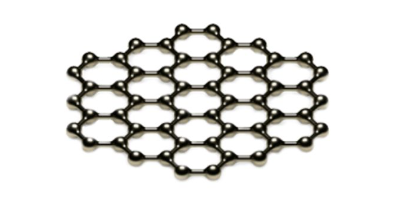
Graphene transducers provide significant benefits for photodetector and sensor products as they can be fabricated directly on CMOS wafers i.e., using single-material platform technology. The key benefit is the ability to monolithically fabricate different graphene-based wavelength-specific detectors on custom designed ROICs through low-temperature post-processing.
Custom CMOS ROICs Design
High performance readout electronics based on Exosens Imaging's patented measurement principles allows significant benefits in designing the next generation solution for our product roadmap including custom ROICs for application specific benefits.
Exosens Imaging designs custom Read-Out Integrated Circuits (ROICs) for VIS-SWIR and thermal detector arrays. This is to ensure best compatibility with novel materials (e.g., graphene) and to enable maximal exploitation of its superlative properties. With this approach, we can create bespoke modular solutions that match our customers’ requirements.
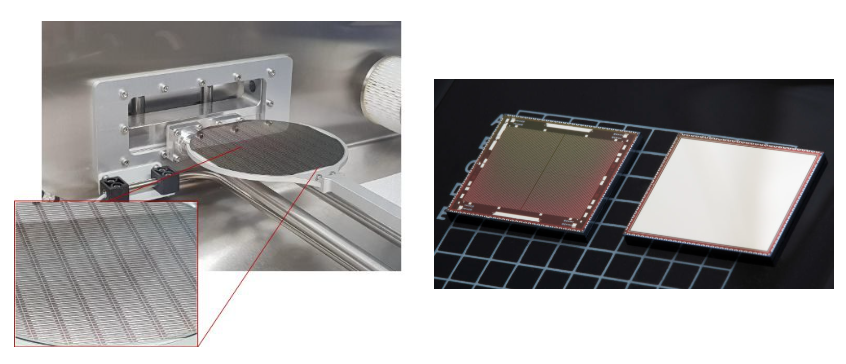
The ROICs are designed for our particular sensor device structures ensuring optimal detector performance and sensor signal quality. With Exosens Imaging's in-house IC design capability, we can cater for customer requirements regarding pixel geometry and architecture in a truly flexible manner. These tailored ROICs are manufactured with conventional CMOS processes available at commercial foundries. We incorporate layers of nanomaterials and graphene monolithically on top of the ROIC wafers leading to a cost-efficient manufacturing process scalable to high production volumes. Our CMOS integrated readout electronics enable the low power consumption and high frame rate necessary for machine vision.
System Integration
Exosens Imaging sensor products are designed for easy integration with the customer’s systems using features of the ROIC and front end electronics:
- Array multiplexing
- Analogue-to-digital conversion
- Global electric shutter
- High Dynamic Range imaging
- Adjustable amplification levels
- Noise reduction and other signal quality enhancements via Correlated Double Sampling
- Custom Design of Front Electronics
- Camera housing design with optimised thermal management
The sensor components are validated to meet the industrial reliability standards (JEDEC). In addition, Exosens Imaging offers measurement modules, which can be utilised for sensor technology evaluation purposes or as reference implementations for product integration. These module boards provide calibrated digital image data output and perform rudimentary low-level image processing steps.
Pyroelectric materials-based sensors (MWIR & LWIR)
Exosens Imaging is also developing MEMS devices in which a suspended pyroelectric substrate structure absorbs thermal radiation and acts as a modulator for the graphene-transistor. These microbolometer devices are sensitive to MWIR and LWIR thermal radiation and can be tuned to be selective to specific spectral ranges by modifying photonics absorbers or antenna structures on the pyroelectric film.
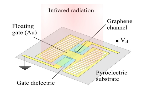
Exosens Imaging is determined to solve challenges faced by the industry with its novel devices using nanomaterials in the mid-wave range and with its high-performance devices enabling:
- MWIR – non-cryocooled
- Lower price of camera compared to existing
- Meeting the specification for applications requiring 3–5 um detection
- Custom ROIC
- Exosens Imaging is exploiting various nanomaterials for its MWIR camera solution.
Beyond state of the art
Multispectral Detectors: Based on similar graphene transducers, it is possible to combine Exosens Imaging VIS-SWIR photodetectors and thermal detectors at the pixel level on a single die creating a multispectral detector array. In this way, Exosens Imaging can cover broad spectral ranges with a single imaging sensor and offer a compact high-performance broadband imaging solution with VIS-SWIR and MWIR/LWIR under one FPA for simultaneous imaging.
The active project will create the basis for super pixel image sensors enabled by GFETs:
- Visible, SWIR and MWIR. Ultimate sensor solution for hyperspectral applications.
- SWIR, MWIR and LWIR. Ultimate detector for surveillance in extreme conditions using simultaneous imaging.
- Visible, SWIR and LWIR. Extremely interesting for defense and surveillance applications.
Exosens Imaging has been pursuing its development with some of its partners
UK MoD, Defence Science and Technology Laboratory (DSTL):
- Technology development of graphene-based image sensors for visible, SWIR and LWIR for simultaneous imaging of three bands
- Development of sensors, ROICs and measurement electronics and software
EU FET Graphene Flagship
- Spearhead project to develop a super pixel camera for hyperspectral industrial applications with separate visible, SWIR and MWIR pixels