
Event
Abu Dhabi.
FROM Feb 17th 2025 TO Feb 21st 2025
International Defence Exhibition and Conference 2025
Visit Exosens at IDEX 2025 Booth 07-A15, in Abu Dhabi
Abu Dhabi.
FROM Feb 17th 2025 TO Feb 21st 2025
Visit Exosens at IDEX 2025 Booth 07-A15, in Abu Dhabi
Technicien QA - Test & Validation H/F
Dec 04th 2025


Ingénieur Commercial International H/F
Dec 04th 2025


May 12th 2025
Enhancing Maritime Surveillance with Advanced Imaging Technology— both day and night. We’re excited to contribute to the MARISPEC research project, aimed at enhancing maritime security.

Apr 15th 2025
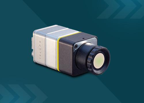
La caméra Radia V60 de Telops — maintenant avec un nouveau mode d’étalonnage haute température


Sep 12th 2024


Nov 25th 2025
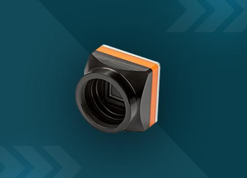
Exosens lance l'Hyper-Cam Airborne Nano, reinventant l'imagerie hyperspectrale infrarouge à ondes longues (LWIR)

Apr 15th 2025
WW Business Development Manager H/F – Non-Destructive Testing (NDT) and Infrastructures Markets
Aug 04th 2025


Nov 25th 2024
In general, infrared detectors are used to detect, image, and measure patterns of the thermal heat radiation which all objects emit or sense reflected light in the non-visible part of the spectrum (just beyond the red). The development of thermocouples and bolometers started in the 19th century. These early devices consisted of single detector elements that relied on a change in the temperature of the detector. The technology has evolved, but the principle of both the bolometer and the thermocouple are still commonly used today.
Thermal detectors are generally sensitive to all infrared wavelengths and operate at room temperature. Under these conditions, they have relatively low sensitivity and slow response.
First Generation Detector Arrays
Photon detectors were developed to improve sensitivity and response time. These detectors have been extensively developed since the 1940’s. Lead sulfide (PbS) was the first practical IR detector. It is sensitive to infrared wavelengths up to ~3 µm.
In the late 1940’s and the early 1950’s, a wide variety of new materials were developed for IR sensing. Lead selenide (PbSe), lead telluride (PbTe), and indium antimonide (InSb) extended the spectral range beyond that of PbS, providing sensitivity in the 3-5 µm medium wavelength (MWIR) atmospheric window.
The end of the 1950’s saw the first introduction of semiconductor alloys, in the chemical table group III-V, IV-VI, and II-VI material systems. These alloys allowed the bandgap of the semiconductor, and hence its spectral response, to be custom tailored for specific applications. MCT (HgCdTe), a group II-VI material, has today become the most widely used of the tunable bandgap materials.
As photolithography became available in the early 1960’s it was applied to make IR sensor arrays. Linear array technology was first demonstrated in PbS, PbSe, and InSb detectors. Photovoltaic (PV) detector development began with the availability of single crystal InSb material.
In the late 1960’s and early 1970’s, “first generation” linear arrays of intrinsic MCT photoconductive detectors were developed. These allowed LWIR forward looking imaging radiometer (FLIR) systems to operate at 80K with a single stage cryoengine, making them much more compact, lighter, and significantly lower in power consumption.
The 1970’s witnessed a mushrooming of IR applications combined with the start of high volume production of first generation sensor systems using linear arrays.
At the same time, other significant detector technology developments were taking place. Silicon technology spawned novel platinum silicide (PtSi) detector devices which have become standard commercial products for a variety of MWIR high resolution applications.
Second Generation Detector Arrays
The invention of charge coupled devices (CCDs) in the late 1960’s made it possible to envision “second generation” detector arrays coupled with on-focal-plane electronic analog signal readouts which could multiplex the signal from a very large array of detectors. Early assessment of this concept showed that photovoltaic detectors such as InSb, PtSi, and MCT detectors or high impedance photoconductors such as PbSe, PbS, and extrinsic silicon detectors were promising candidates because they had impedances suitable for interfacing with the FET input of readout multiplexers. PC MCT was not suitable due to its low impedance.
Therefore, in the late 1970’s through the 1980’s, MCT technology efforts focused almost exclusively on PV device development because of the need for low power and high impedance for interfacing to readout input circuits in large arrays. This effort has been paying off in the 1990’s with the birth of second generation IR detectors which provide large 2D arrays in both linear formats. These detectors use TDI for scanning systems; in staring systems, they come in square and rectangular formats.
Monolithic extrinsic silicon detectors were demonstrated first in the mid 1970’s. The monolithic extrinsic silicon approach was subsequently set aside because the process of integrated circuit fabrication degraded the detector quality. Monolithic PtSi detectors, however, in which the detector can be formed after the readout is processed, are now widely available.
Later, the introduction of different III-V material alloys enables detection in other spectral bands: For example, InGaAs sensitive in the SWIR (Short Wave InfraRed) band allowing a different type of applications and benefits. In most cases, InGaAs operates at room temperature.
More recently, new materials emerged, opening new applications areas for InfraRed detectors and imagers.
Jan 23rd 2025
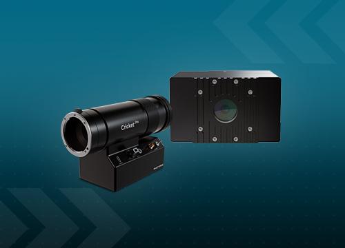
Photonis launches Cricket™ pro and PhotonPix™: Two market-leading solutions...
In general, infrared detectors are used to detect, image, and measure patterns of the thermal heat radiation which all objects emit or sense reflected light in the non-visible part of the spectrum (just beyond the red). The development of thermocouples and bolometers started in the 19th century. These early devices consisted of single detector elements that relied on a change in the temperature of the detector. The technology has evolved, but the principle of both the bolometer and the thermocouple are still commonly used today.
Thermal detectors are generally sensitive to all infrared wavelengths and operate at room temperature. Under these conditions, they have relatively low sensitivity and slow response.
First Generation Detector Arrays
Photon detectors were developed to improve sensitivity and response time. These detectors have been extensively developed since the 1940’s. Lead sulfide (PbS) was the first practical IR detector. It is sensitive to infrared wavelengths up to ~3 µm.
In the late 1940’s and the early 1950’s, a wide variety of new materials were developed for IR sensing. Lead selenide (PbSe), lead telluride (PbTe), and indium antimonide (InSb) extended the spectral range beyond that of PbS, providing sensitivity in the 3-5 µm medium wavelength (MWIR) atmospheric window.
The end of the 1950’s saw the first introduction of semiconductor alloys, in the chemical table group III-V, IV-VI, and II-VI material systems. These alloys allowed the bandgap of the semiconductor, and hence its spectral response, to be custom tailored for specific applications. MCT (HgCdTe), a group II-VI material, has today become the most widely used of the tunable bandgap materials.
As photolithography became available in the early 1960’s it was applied to make IR sensor arrays. Linear array technology was first demonstrated in PbS, PbSe, and InSb detectors. Photovoltaic (PV) detector development began with the availability of single crystal InSb material.
In the late 1960’s and early 1970’s, “first generation” linear arrays of intrinsic MCT photoconductive detectors were developed. These allowed LWIR forward looking imaging radiometer (FLIR) systems to operate at 80K with a single stage cryoengine, making them much more compact, lighter, and significantly lower in power consumption.
The 1970’s witnessed a mushrooming of IR applications combined with the start of high volume production of first generation sensor systems using linear arrays.
At the same time, other significant detector technology developments were taking place. Silicon technology spawned novel platinum silicide (PtSi) detector devices which have become standard commercial products for a variety of MWIR high resolution applications.
Second Generation Detector Arrays
The invention of charge coupled devices (CCDs) in the late 1960’s made it possible to envision “second generation” detector arrays coupled with on-focal-plane electronic analog signal readouts which could multiplex the signal from a very large array of detectors. Early assessment of this concept showed that photovoltaic detectors such as InSb, PtSi, and MCT detectors or high impedance photoconductors such as PbSe, PbS, and extrinsic silicon detectors were promising candidates because they had impedances suitable for interfacing with the FET input of readout multiplexers. PC MCT was not suitable due to its low impedance.
Therefore, in the late 1970’s through the 1980’s, MCT technology efforts focused almost exclusively on PV device development because of the need for low power and high impedance for interfacing to readout input circuits in large arrays. This effort has been paying off in the 1990’s with the birth of second generation IR detectors which provide large 2D arrays in both linear formats. These detectors use TDI for scanning systems; in staring systems, they come in square and rectangular formats.
Monolithic extrinsic silicon detectors were demonstrated first in the mid 1970’s. The monolithic extrinsic silicon approach was subsequently set aside because the process of integrated circuit fabrication degraded the detector quality. Monolithic PtSi detectors, however, in which the detector can be formed after the readout is processed, are now widely available.
Later, the introduction of different III-V material alloys enables detection in other spectral bands: For example, InGaAs sensitive in the SWIR (Short Wave InfraRed) band allowing a different type of applications and benefits. In most cases, InGaAs operates at room temperature.
More recently, new materials emerged, opening new applications areas for InfraRed detectors and imagers.

Camp de Souge.
FROM Apr 02nd 2025 TO Apr 04th 2025

Sep 29th 2025

Jul 22nd 2024

Feb 17th 2023

Jun 24th 2015

Jul 21st 2023
Photonis a global leader of electro-optical detection and imaging technologies for defense and industrial markets, held by HLD since 2021, announced today the acquisition of Israeli company El-Mul
Aug 01st 2024
Jun 03rd 2025
Stay connected
Stay informed and connected to the latest news from Exosens by signing up.