Thermal imaging can be a very powerful tool for semiconductor failure analysis. Current leakage defects typically generate thermal hot-spots: metal short circuits, latch-up, junction defects in diodes and transistors, breakdown of MOS gate oxide, ESD failures, etc. When using conventional thermography or thermal imaging on semiconductor devices, we are faced with two problems:
- Intensity variations caused by differences in emissivity of the various materials;
- Thermal hot spot dilation – heat will spread out from defect location.
Differences in emissivity
When using a thermal camera to inspect semiconductor devices, one can see a contrast in the infrared image even when no bias voltage is applied, i.e., the device or wafer is at a uniform temperature. This contrast is caused by differences in emissivity of the materials in the semiconductor device, as shown in Figure 1 as an example.
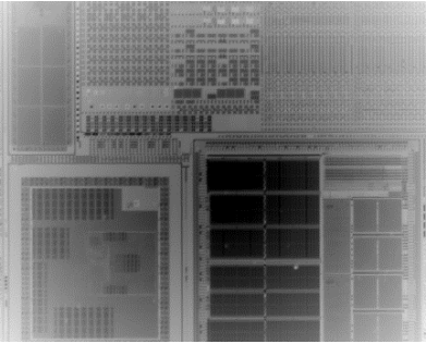
Figure 1 Emissivity-contrast: structure of a device on wafer, imaged through 780 μm thick silicon substrate. Image courtesy of SEMICAPS Pte Ltd.
The high thermal conductivity of silicon causes low thermal gradients across powered devices. Heat sources in silicon are often imaged as a large blob. The sensitivity of the camera also picks up the changes in emissivity with the temperature of the different materials in the device. This shows up as an image of the device in the thermal emission image, despite background correction between a powered and unpowered state of the device.
Thermal hot spot dilation
Thermal hot spot dilation is heat spreading from the defect location. The problem with thermal hot spot dilation is even more acute when a point heat source is located below the surface, i.e., when imaging through the silicon substrate. The thermal hot-spot is ‘lost’ within a larger dilated area.
Lock-in thermal imaging
Lock-in thermal imaging uses pulsed electrical stimulation on the semiconductor device, and a thermal camera, synchronized to the timing of the power supply, to minimize thermal hot spot dilation. Lock-in thermal imaging results in improved defect localization accuracy and thermal sensitivity.
Moreover, phase delay information from thermal lock-in analysis (thermal time delay will cause a phase shift, see Figure 2 and Figure 3) can be used to determine the location of a hot spot or failure in a 3D structure of stacked integrated circuits. As shown schematically in Figure 2, conventional thermal imaging methods would be unable to distinguish differences in depth location between the two heat points (or failure sources).
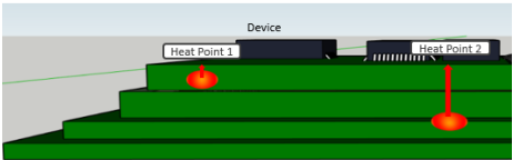
Figure 2 Heat points on a 3D structure or stacked device.
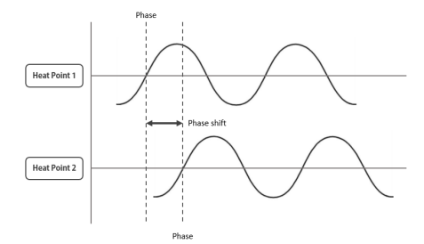
Figure 3 Using the difference between the phases of Heat Points 1 & 2 (see Figure 2), the depth of the respective failure points can be calculated.
Figures 4 and 5 show an example of lock-in thermal imaging (without using any phase information). Figure 4 is the thermal lock-in image and it shows the faint signal of a hot spot dissipating 2 μW of power (device is biased at 1 V and 2 μA). Figure 5 is the overlay image – thermal emission (from lock-in image, and in pseudo-color and after thresholding) is superposed on a thermal background image.
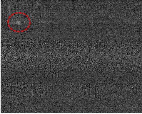
Figure 4 Lock-in thermal emission image of a hot spot. Image courtesy of SEMICAPS Pte Ltd.
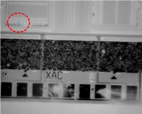
Figure 5 Overlay of thermal emission on the thermal background image. Image courtesy of SEMICAPS Pte Ltd.
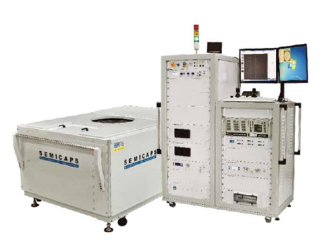
Figure 6 The SEMICAPS SOM5000 Tester Docked Wafer Prober Thermal Microscope System by SEMICAPS Pte Ltd.
The above example demonstrates the value and effectiveness of using thermal lock-in when conducting semiconductor inspections. The ability to localise defects reduces the time required for failure analysis engineers to identify and rectify the issue. The overall efficiency of a wafer level inspection process is improved thanks to thermal lock-in enabled by the Xenics XCO 640 camera module. The XCO camera module is used in the SEMICAPS SOM5000 Tester Docked Wafer Prober Thermal Microscope System.
The XCO 640 is based on a cooled MWIR engine that offers the following advantages:
- Versatility – small size and open frame camera module
- F/2 aperture (others available)
- Low NETD (Noise Equivalent Temperature Difference) of 25 mK
- Choice between InSb (3.6 to 4.9 μm) or MCT (3.7 to 4.8 μm) detectors
- High sensitivity and high resolution detector with 15 μm pixel size
- GigE vision or CameraLink data and trigger interface
The XCO 640 camera module is also used in the Xenics Tigris camera family for scientific applications. The Tigris camera comes with a compact housing, a bayonet mount for a range of standard (non-microscope) lenses and a filter wheel.
Documentation
Application Note


Related content

Munich.
FROM Nov 10th 2026 TO Nov 13th 2026
SEMICON EUROPA 2026
Join Exosens at SEMICON EUROPA 2026 2026 in Munich

Edinburgh.
FROM Sep 14th 2026 TO Sep 17th 2026
SPIE Sensors + Imaging 2026
Join Exosens at SPIE Sensors + Imaging 2026 Edinburgh, United Kingdom

Jul 07th 2026
Multifocal Femtosecond Laser Writing
Crosstalk Limits in Multifocal Parallel Femtosecond Direct Laser Writing: Decoherence Strategies and Quantitative Validation of Nanostructure Optical Phase

Jun 29th 2026
Exosens secures contract with BROLIS
Exosens secures major long-term contract with BROLIS to supply 17000 high-performance image intensifier tubes for the Czech Armed Forces

Aug 20th 2021
Visit our booth #514 during OPTIFAB

Jun 25th 2026
Strengthening Defense & Security Innovation
Exosens secures €140 million in EIB financing to foster innovation in Europe’s defense and security industry