I need to survey my offshore facility and underwater installations. Is it still possible to detect methane?
Yes! Our hyperspectral imaging technology works even over water.
Photonis, Xenics and El-Mul are now unified under the Exosens brand. Read more →
I need to survey my offshore facility and underwater installations. Is it still possible to detect methane?
Yes! Our hyperspectral imaging technology works even over water.
If I need to survey my facility during winter time, is snow a problem?
Not at all! Our methane detection solution works, whether in daylight or nighttime, and even over snow!
Do you have any certification for your methane detection solution?
Yes! Our methane airborne detection solution has been officially documented as an emission detection method by the Alberta Methane Emissions Program (AMEP) to be included in an Alternative Fugitive Emissions Management Program. You can have all details here : https://www.exosens.com/news/amep-telops

Oct 27th 2025
Exosens achieves a strong 9M 2025 performance driven by continued defense tailwinds
Colorado .
FROM Oct 08th 2025 TO Oct 09th 2025
Join Exosens at the 12th annual CH4 Connections 2025 conference in Fort Collins, Colorado

Oct 14th 2025
HLD Europe yesterday announced that it has entered into an agreement with Theon International, the Group’s main customer, for the sale of 9.8% of Exosens’ share capital...
Oct 09th 2025
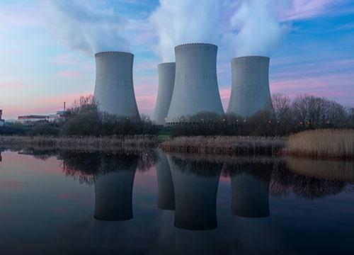
Proven reliability up to 800°C and beyond for SMR and AMR applications. Built on the combined legacy of Photonis and Centronic—80+ years of neutron detection excellence.
Paris.
FROM Nov 18th 2025 TO Nov 21st 2025
Join Exosens at Milipol Paris 2025, the world’s leading event for homeland security and safety, taking place at Parc des Expositions Nord Villepinte in Paris, France.
Oct 06th 2025
Exosens makes on-site neutron radiography accessible with portable detection solutions, enabling non-destructive testing in nuclear and industrial environments.
Coronado Springs Resort and Convention Center .
FROM Oct 06th 2025 TO Oct 09th 2025
Join Exosens at ASNT 2025 Annual Conference - Coronado Springs Resort and Convention Center – Orlando, FL Booth: #1128
Stay connected
Stay informed and connected to the latest news from Exosens by signing up.