In this article, we discuss several applications of SWIR (short-wave infrared) cameras in infrared semiconductor inspection applications. Most of these applications rely on the capability of SWIR cameras to see through semiconductor materials such as silicon.
Introduction
The semiconductor industry has grown to become one of the largest industries in the world. Semiconductor industry covers a wide variety of applications, ranging from processor and memory integrated circuits for PCs or mobile devices, to solar cells.
In the semiconductor industry, SWIR cameras can be used to inspect the quality of pure semiconductor material (usually silicon) after ingot growth. Furthermore, ingots that are subsequently sliced into wafers and these wafers can in a similar way be inspected for defects or cracks. Wafers are then processed into (opto-) electronic components. For semiconductor devices, the final processing step is dicing of the wafer into single chips – and here a SWIR camera is used for alignment of the saw blade or laser.
In order to do failure analysis, fabricated integrated circuits can undergo microscope inspection for cracks, or photon emission. Three-dimensional MEMS (micro-electromechanical systems) structures require inspection throughout the production process.
For all these applications, Xenics offers a wide range of SWIR cameras, both for two-dimensional (2D) and linescan imaging. SWIR cameras typically use Indium Gallium Arsenide (InGaAs) based detectors and have a high response (quantum efficiency) in the 900 to 1700 nm wavelength range, ideally suited for imaging through or inside silicon.
Silicon ingot and brick inspection
SWIR InGaAs cameras (both 2D and linescan) are widely used in the semiconductor industry for the inspection of crystalline silicon (Si) bricks or ingots. Impurities and inclusions inside the brick or ingot can easily be detected using a SWIR camera and a light source emitting with a wavelength longer than 1150 nm (see example image in Fig. 1). The reason for this is that the bandgap in this semiconductor material (Si) does not absorb the lower energy and longer wavelength SWIR photons, whereas visible photons (which have higher energy) are absorbed. This makes SWIR InGaAs cameras an excellent inspection tool that allows straightforward detection of impurities, defects, voids or inclusions.
The impurities inside the brick or ingot can cause damage to the production equipment when the ingots are further processed into wafers. SWIR cameras can avoid this problem and consequently ensure a smooth production process and higher efficiency.
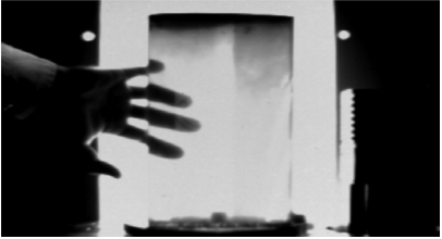
Fig. 1: SWIR InGaAs picture of a Si brick – note that the ingot is completely transparent for SWIR radiation.
For this application, Xenics mainly offers Bobcat 640 and Xeva 640 cameras, and also high resolution linescan Lynx 2048 cameras.

Fig. 2: Cameras suitable for Silicon ingot and brick inspection: Bobcat 640, Xeva 640, and the Lynx.
Wafer and die inspection
Imaging through semiconductor wafers and integrated circuit chips for defect inspection is easy and straightforward when using a SWIR camera because these materials (Si and Gallium Arsenide (GaAs)) are transparent in the short-wave infrared wavelength range. This ability to see through Si, the most commonly used semiconductor material by far, provides a non-destructive inspection method greatly improving the production process.
During the wafer manufacturing process, particles or cracks can exist inside or between wafers. Whereas visible CCD or CMOS cameras can be used to detect defects on top of a wafer, SWIR cameras have the capability to see “inside” Si and can detect particles, voids or other imperfections between two bonded wafers.
Die inspection before packaging is also a common application for SWIR cameras as they can see small cracks, caused by wafer dicing, hidden inside the Si material (see example image in Fig. 3).
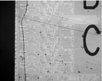
Fig. 3: Inspection of a die side – looking for dicing damage inside Si. Image taken with SWIR InGaAs camera.
SWIR cameras are used to improve yield in MEMS manufacturing: sealing inspection (detection of bubbles or breaches; see example image in Fig. 4), device defect inspection, critical dimension and overlay measurement. For wafer level packaging (WLP), a technique combining wafer manufacturing and device encapsulation technologies, SWIR cameras are used for multiple quality assessment tasks. Using WLP, many integrated circuits can be stacked together using interconnect processes like TSV (through-Si via) or metal bumps, followed by encapsulation [MUE].
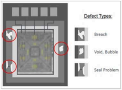
Fig. 4 : Short-wave infrared image showing hermeticity fail [MUE]
For these applications, Xenics offers a variety of suitable cameras: Bobcat 320 and Bobcat 640, Xeva 320 and Xeva 640.
Photon emission
Short-wave infrared photon emission microscopy (PEM) is an established, passive, fault localization technique for microelectronic failure analysis. Photon emission occurs when an electron makes a transition from a higher energy state, to a lower energy state. All or part of the energy difference is emitted as electromagnetic radiation. Photon emission from defects are generally associated with forward and reverse biased pn junctions, transistors in saturation or dielectric breakdown [REV]. An example SWIR image overlaid with an emission SWIR image is shown in Fig. 5.
Nowadays, mainly (highly-sensitive, cooled) SWIR cameras are used for PEM, because:
- Si CCD cameras are only effective for observing photon emissions with energy transitions above the Si bandgap;
- Si CCD cameras do not allow the observation of intra-band emissions;
- sub-bandgap emissions involving chemical impurities, physical defects and deep traps and other recombination centers are also not observable;
- backside analysis (necessary with the use of multi-level metals preventing photon emission from front side of wafer) requires transmission of the emission through the Si substrate
Especially the Xenics Cougar camera and the 3-stage TEC cooled versions of Xeva and Cheetah cameras are suitable for this application.
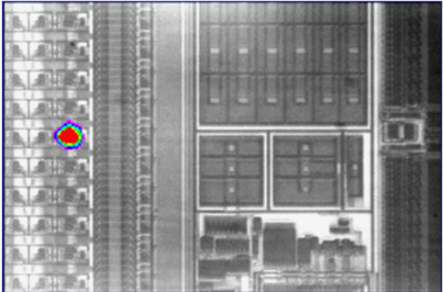
Fig. 5: Photon emission image superimposed on a chip layout image – images taken through backside of wafer with a SWIR InGaAs camera.
Photovoltaic wafer inspection – EL & PL
Solar cell crack inspection or efficiency mapping is usually based on the luminescence effect, i.e., emission of light from a semiconductor material when electrons transition from an excited state to the ground level state. Their excess energy is turned into photons and their wavelength is determined by the bandgap of the solar cell absorption material – for Si this bandgap energy corresponds to a wavelength of about 1150 nm. Note also that in case the Si material contains some defects, the peak value is smaller and the emission occurs with a lower energy level (sub-bandgap) in the defect band at longer wavelengths between 1300 and 1600 nm [SWI]. An example image is shown in Fig. 6. Other materials such as Copper Indium Gallium di-Selenide (CIGS) or Copper Indium di-Selenide (CIS) can also be used for solar cell production. For these materials, the emission peak wavelength is above 1300 nm.
Two methods can be used for luminescence imaging: electroluminescence (EL) or photoluminescence (PL). For EL, the excitation is done by applying a current. For PL, (shorter wavelength) light excitation is used to provoke the emission, and the shift between absorption and emission wavelength (Stokes shift) causes emission in the near and short-wave infrared.
EL inspection can be deployed only in the last manufacturing step. Only at this stage, an external voltage can be applied to inject electrons into the manifold pn-junctions which form the solar cell. Therefore, the EL method is only feasible on completely processed, finished and metalized solar cells. There is no way for characterization at the preceding steps of the manufacturing process, as no electrical contacts are available.
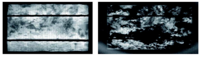
Fig. 6: On the left is a luminescence image of solar cell taken with SWIR InGaAs camera and bandpass filter centered around 1100 nm. On the right is the same solar cell, picture taken with same SWIR InGaAs camera but now using a long-wave pass filter (transmitting above 1450 nm), showing the defect luminescence [SWI].
In summary, the advantages of PL with SWIR, over EL with SWIR or CCD cameras, are:
- It allows wafer characterization showing the spatial resolution at all solar cell manufacturing steps. Images of silicon blocks and singulated wafers at various stages of the manufacturing process can be analysed for an early estimation of the expected quality of the finished solar cell.
- PL is a contactless technique. PL inspection is performed without contacting the material being inspected.
- SWIR cameras have high QE at the emission wavelengths and inspection can be done, in-line at video rate, unlike Si based CCD cameras that require exposure times up to several seconds.
Therefore, PL imaging has great potential as an in-line monitoring tool for Si blocks, ingots, raw wafers, partially finished or finished wafers [SOL].
Xenics cameras suitable for this application are Xeva 640 and Bobcat 640
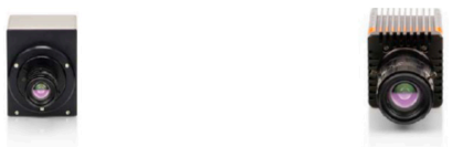
Fig. 7: SWIR cameras Xeva 640 (left) and Bobcat 640 (right)
Crack detection using linescan SWIR cameras
Detection of cracks and micro-cracks as early as possible in the production process has become very important. Cracks in the fragile semiconductor material can cause breakage of individual solar cells, and production machine downtime.
Instrumentation for in-line crack detection is a part of today’s standard production lines of solar cells. However, automatic crack detection in crystalline Si wafers, especially multi-crystalline, can be a challenging task. Some of the challenges are:
Detection of small cracks (micro-cracks): a small crack present in a wafer acts as an initiation centre for crack growth
Image intensity variations due to varying crystal grain orientation and wafer thickness
Inspection speed matching the wafer line cycle time
A relatively new crack detection technique is based on a transflection illumination technique. Transflection is a combination of reflection and transmission. It is the optical phenomenon when light entering a (partly) transparent object is scattered and exits from the object at a different position from the point of entrance.
This transflection method addresses some important challenges in automated crack detection. The main features of the transflection method are:
The wafer is illuminated through the wafer surface – light source and camera are positioned on the same side of the wafer
Light is reflected by cracks in the wafer. Cracks will block the light transport. Beyond the crack the light intensity inside the wafer will be significantly lower and the surface luminance will be strongly reduced.
The imaged wafer area is separated from the illuminated are by some distance
For small cracks or micro-cracks, the main advantage of this technique is that the crack will cast a shadow, creating a crack signature that is much larger than the crack. Xenics cameras suitable for this application are the Lynx 2048 and 1024 (see example image in Fig. 8).
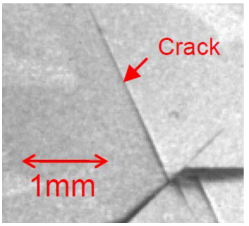
Fig. 8: SWIR InGaAs image of a small crack in a Si wafer. Image taken using broadband light [TRA].
No need for SWIR InGaAs cameras?
Nowadays, many reasonably priced CCD and CMOS cameras can also be used for solar cell inspection. Some suppliers of Si based CCD and CMOS cameras even offer products specifically developed for inspection of solar cells. These special near-infrared CCD or CMOS cameras offer an extended wavelength response beyond 1000 nm – just enough to see the shortest wavelengths emitted by Si electro- or photoluminescence.
In addition to the lower cost compared to InGaAs cameras, the low noise, high resolution and wide dynamic range of these sensors are clear advantages. However, the disadvantage is the need for long integration times (several seconds), and therefore, these cameras can only be used for offline inspection.
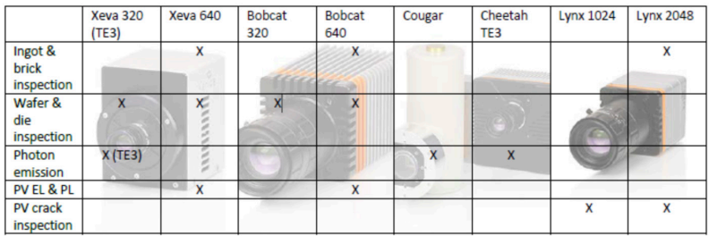
Table 1: Overview of applications in semiconductor inspection and suitable Xenics SWIR cameras
References
[SWI] SWIR Photoluminescence Testing – Raf Vandersmissen, Xenics, Application Note, Belgium.
[SOL] Solar cell inspection via photoluminescence imaging in the NIR/SWIR – Princeton Instruments, Application Note, USA.
[TRA] Transflection, a new illumination technique for in line crack detection in crystalline silicon wafers – Lars Johnsen, SINTEF ICT, Norway.
[REV] A Review of Near Infrared Photon Emission Microscopy and Spectroscopy – JCH Phang, Proceedings of 12th IPFA 2005, Singapore.
[MUE] www.muetec.com – Germany.
Documentation
Application Note


Related content

Munich.
FROM Nov 10th 2026 TO Nov 13th 2026
SEMICON EUROPA 2026
Join Exosens at SEMICON EUROPA 2026 2026 in Munich

Edinburgh.
FROM Sep 14th 2026 TO Sep 17th 2026
SPIE Sensors + Imaging 2026
Join Exosens at SPIE Sensors + Imaging 2026 Edinburgh, United Kingdom

Jul 07th 2026
Multifocal Femtosecond Laser Writing
Crosstalk Limits in Multifocal Parallel Femtosecond Direct Laser Writing: Decoherence Strategies and Quantitative Validation of Nanostructure Optical Phase

Jun 29th 2026
Exosens secures contract with BROLIS
Exosens secures major long-term contract with BROLIS to supply 17000 high-performance image intensifier tubes for the Czech Armed Forces

Aug 20th 2021
Visit our booth #514 during OPTIFAB

Jun 25th 2026
Strengthening Defense & Security Innovation
Exosens secures €140 million in EIB financing to foster innovation in Europe’s defense and security industry