Silicon photodiodes are the basic building block of the majority of modern light detectors. Exosens’s discrete and array photodiodes provide engineers with direct access to the most immediate, intimate signals from the diode junction for applications where speed, sensitivity and precision are of the highest importance. This is in contrast to other, more integrated, devices in which photodiodes are typically buried deep inside behind signal processing and addressing circuitry.
Learn more about Silicon photodiodes
Besoin de précisions ? Contactez nos experts !
Contactez-nousStandard photodiodes
Standard combinations
Custom combinations
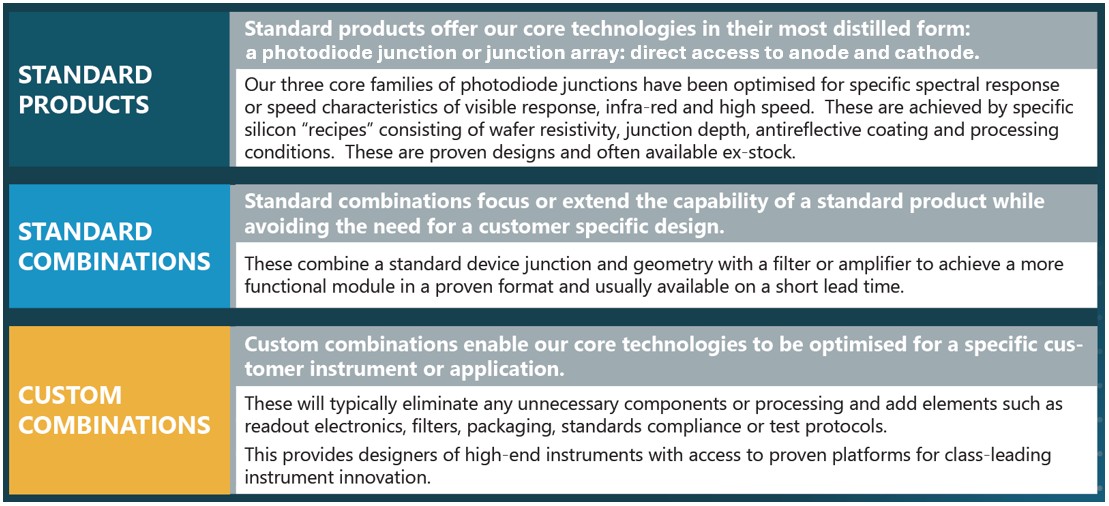
Standard photodiodes
Standard silicon photodiodes : PN and PiN photodiode junctions for sensitivity, speed and spatial precision
Lire la suiteStandard combinations
Standard silicon photodiode combinations : PiN photodiodes combined with a filter or amplifer
Lire la suiteCustom combinations
Custom silicon photodiode combinations : PN and PiN photodiodes in unique geometries and combinations for customer's specific instruments
Lire la suiteLearn more about Silicon photodiodes
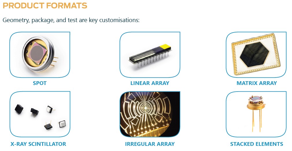
Standard photodiodes are widely used in spot or linear array formats to detect or measure light in the UV, visible and near infrared wavelengths for industrial, metrology, medical and military applications including counting, ambient light measurements and basic position sensing. Standard combinations add funtionality to the diode by integrating a filter or amplifier in an easy to use unit without incurring delays or engineering costs.
Engineers value the robustness and and well understood performance of the silicon photodiode coupled with the longstanding operating experience of Exosens's standard junctions.
Purchasing managers appreciate the proven manufacturing processes which deliver modern silicon photodiodes supported by Exosens’s expertise in achieving enduring availability and continuity of supply as a highly focussed detector manufacturer.
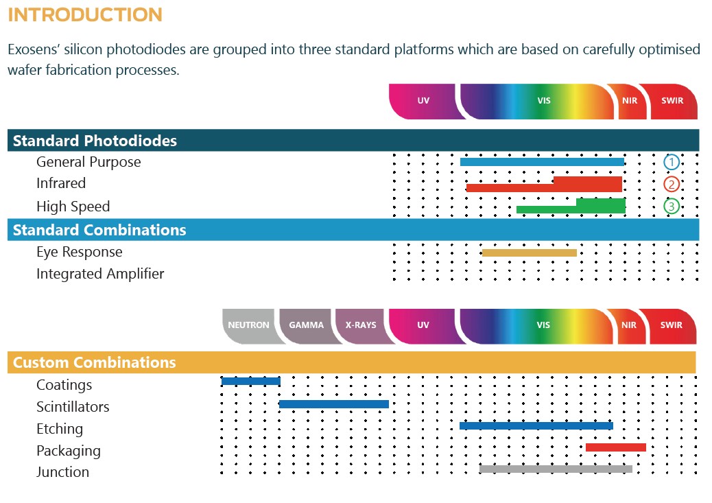
Exosens silicon photodiodes are offered as three product platforms and three levels of integration:
Standard product platforms
Our three silicon photodiode platforms are each optimised for different characteristics. This is primarily achieved by using different silicon specifications and junction depths.
> General Purpose
• ~230nm to 1100nm
> Infrared
• Enhanced response and speed in the 800nm to 1064nm region
> High speed
• Epitaxial devices for <1ns response
Standard combinations
Two commonly encountered requirements can be fulfilled by our off-the shelf combinations:
> Eye response / photopic response
• our general purpose photodiode is combined with an appropriate filter
> Integrated amplifier
• a detector, typically infrared, is combiend with an op-amp die in a standard TO package
Custom combinations
When an application or instrument requires ultimate performance to be acheived by optimising a particular parameter, our standard devcies and combianations serve as a platform on which customisations can be developed with maximum flexibiilty and minimum risk.
While every project and customer is different, typical examples include:
> Military designators, countermeasures and fuses
• high sensitivity, high speed infrared detectors packaged and qualified for harsh environments
> Medical x-ray dosimetry
• a photodiode intimately bonded to a scintillator and packaged to prevent light ingress
> Laser diffraction arrays
• high density photodiode arrays processed to minimise reflection, scatter and peripheral collection
Many instrument designers are experienced in selecting and deploying silicon photodiodes however we recognise that for some engineers this technology may be less familiar. In both cases we strongly encourage users to engage with us at the earliest opportunity in their design process.
In a photodiode the sensor consists of a carefully formed junction within the silicon wafer.
- A PN or PiN junction is created in the silicon wafer by ion implantation of dopants
- This creates a neutral (depletion) region where almost all charge carriers have been expelled by the fixed charges arising from the dopants
- When light is absorbed in the depletion region it excites charge carriers (electrons...) which can move efficiently because they are the only mobile charges present
- These charge carriers are collected at the electrodes (anode and cathode)
- In this way the photodiode absorbs lights and generates an immediate electric signal (pulse or current)